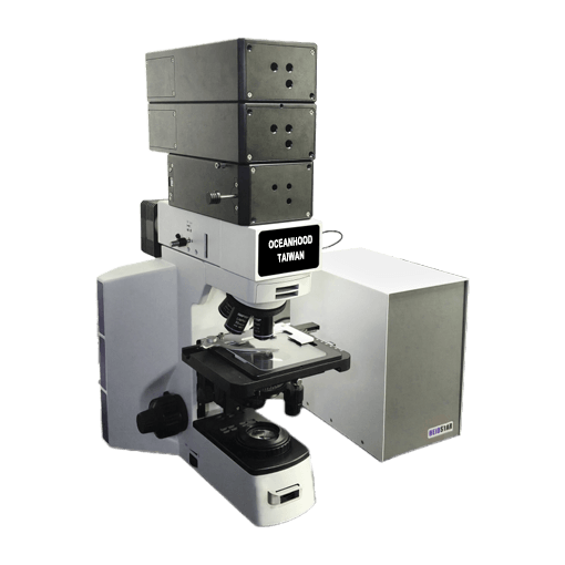
Conventional fiber optic probes used for transmission and reflectance measurements are limited by the size of the illumination spot, with a minimum sampling diameter typically ranging from 1 to 2 mm. This limitation reduces spatial spectral resolution and restricts effective analysis of microscopic sample regions. To address these limitations and meet the growing demand for microscale optical characterization, the Micro Transmittance and Reflectance Spectroscopy System integrates spectroscopy with microscopic optics to acquire spectral information from micron-scale regions.
The system adopts a fiber-optic confocal illumination design. Compared with conventional Köhler illumination, the confocal configuration provides higher focusing accuracy and a smaller sampling spot, significantly improving spatial spectral resolution. Users can select a target area directly under the microscope and obtain its reflectance or transmission spectrum in real time.
The system is widely used in materials science, microelectronics, biological tissues, chemical analysis, optical thin films, semiconductor chips, and related fields. It is an effective tool for investigating surface uniformity, localized optical properties, and spectral responses of microstructures, making it well suited for research institutes, university laboratories, and advanced material inspection applications.
-
Features
- Modular design
Spectroscopy measurements can be achieved by adding an expansion module to the microscope. Customized detection modules can also be developed for customers' existing microscope systems. - Confocal optical design
The illumination path and the optical path for spectrum collection are coaxial, and the unique confocal design ensures that the measurement directly corresponds to the area of interest, effectively suppressing stray light. - Wide spectral measurement range
Combined with Oceanhood fiber optic spectrometers, the system supports broadband measurements from 350–1700 nm. - Flexible configuration and upgrade
In addition to transmission and reflectance measurements, the system can be expanded with dedicated measurement modules to perform transmission, reflectance, Raman, and fluorescence multispectral measurements. - High-precision measurement
The automated motorized stage features a minimum step size of 1 μm, enabling spectral scanning of microscopic regions.
-
Specifications
| Spectral module | |
| Spectral range | 350–1700 nm |
| Spectral resolution | 2–8 nm |
| Spatial resolution | 12 μm @ 50X objective, minimum 2 μm |
| Detector | Back-illuminated area-array CCD and InGaAs detector, both TE-cooled |
| Microscope module | |
| Objective lenses | Infinity-corrected long working distance plan achromatic metallurgical objectives, 10X, 20X, 50X; optional NIR objectives |
| Nosepiece | Built-in four-position objective turret |
| CCD imaging | 9 MP color camera |
| Motorized stage (with Mapping | Travel: 80 mm × 60 mm; Resolution: <0.05 μm; Maximum speed: 50 mm/s; Unidirectional repeatability: ≤1 μm; Bidirectional repeatability: ≤2.5 μm; Absolute positioning accuracy (10 mm): ≤±2 μm |
| Focusing mechanism | Coaxial coarse and fine focusing with travel limit and locking mechanism; Coarse adjustment: 30 mm/revolution; Fine adjustment scale: 2 μm |
| Incident light illumination system | 12 V / 60 W halogen lamp with adjustable brightness |
-
Measurement examples
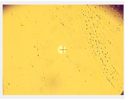
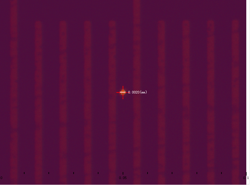
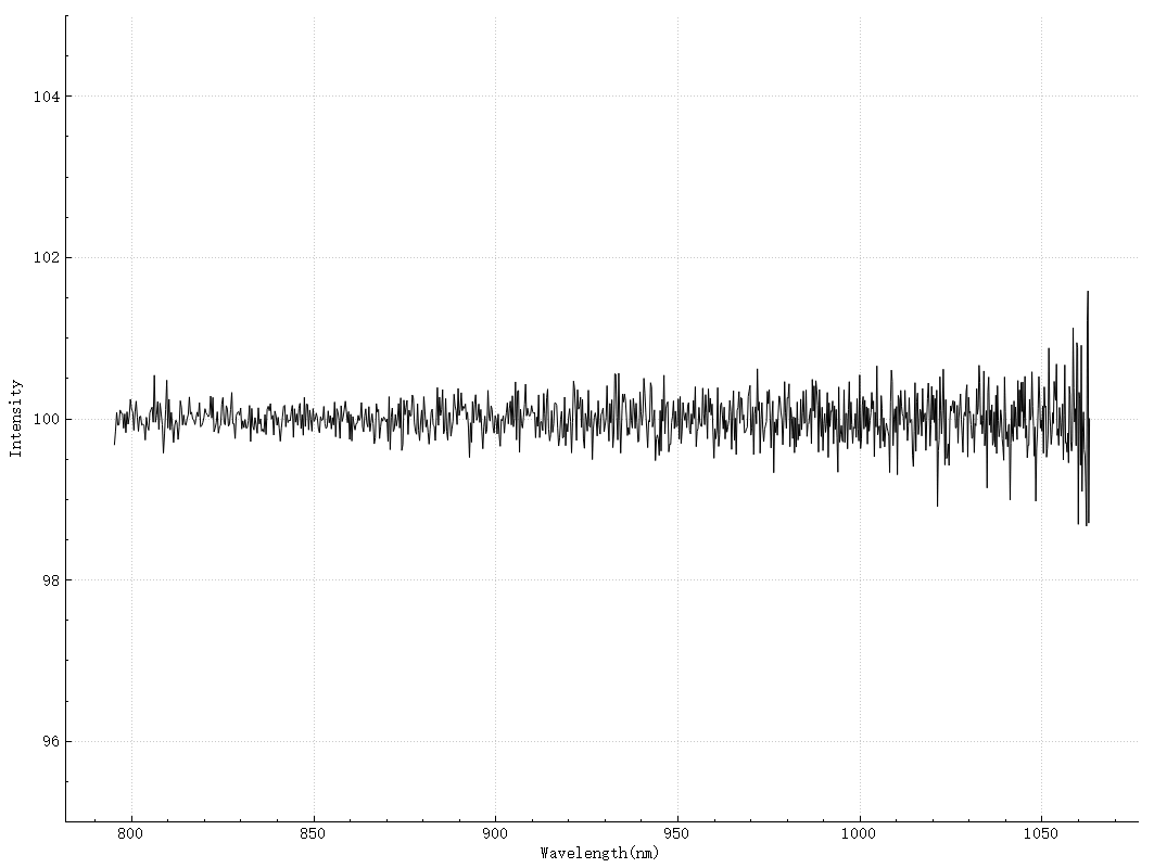
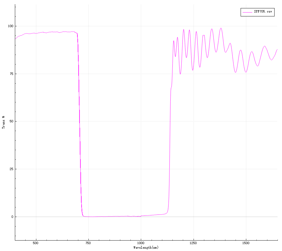
Minimum sampling spot
-
Applications
With high spatial resolution spectral acquisition, the system enables detailed analysis of samples from the micrometer to nanometer scale. It provides high-precision characterization of chemical composition, molecular structure, crystal structure, and thin-film thickness.
The system is suitable for research and development of advanced materials, thin-film technologies, optoelectronic devices, coated lenses, and various optical components requiring transmission and reflectance characterization.
Micro-area transmission and reflection Mapping is a high-precision analytical technique that focuses light onto microscopic regions of a sample through the microscope system and collects transmission and reflectance spectra from each point. By performing point-by-point scanning across the sample surface, spectral images of the entire sample area can be generated to obtain two-dimensional or three-dimensional spectral distribution information. This enables transmission and reflectance characterization at the microscopic scale.
The technique is widely applied in materials science, chemical analysis, biomedical research, forensic science, and environmental monitoring.
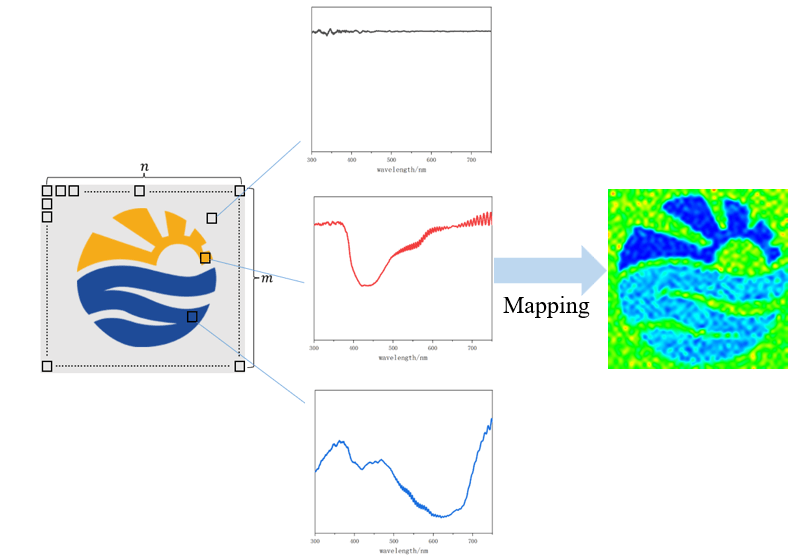
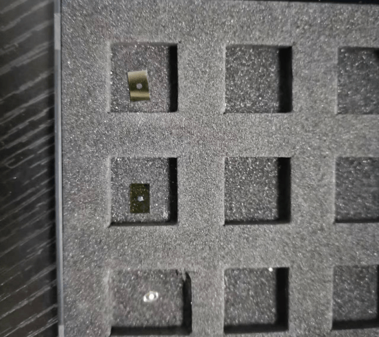
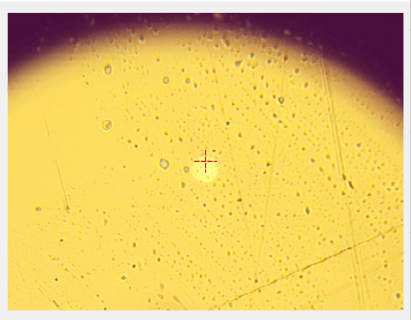
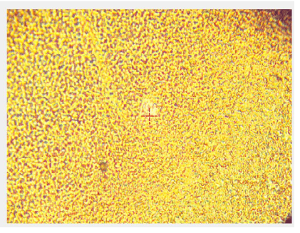
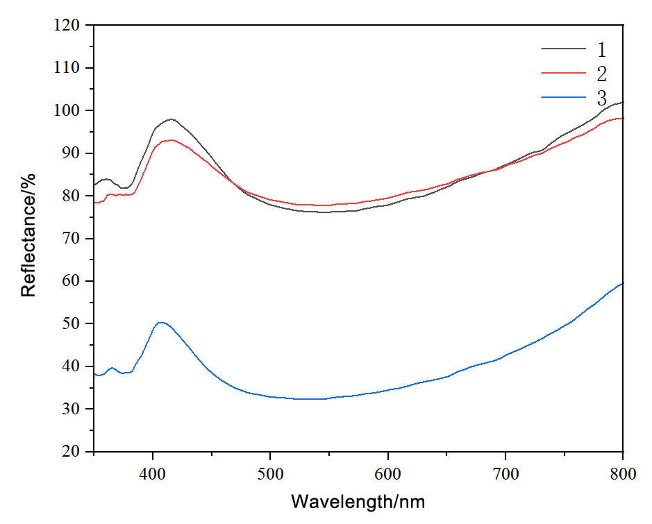
Application example – Micro-area reflectance measurement of coated chips